
Applications
 Part of the Oxford Instruments Group
Expand
Collapse
Part of the Oxford Instruments Group

Application Notes
Published: 01 Jul 2025 · Last updated: 03 Aug 2026
Correlative imaging techniques gain more and more importance in many fields of applications due to the fact that more characteristics of a specimen can be analyzed with one instrument. The efficient workflow of correlative microscopy techniques is an additional advantage that saves time and money. In this application note we present correlative RISE microscopy: the first instrument combining a fully loaded SEM with a confocal Raman microscope including white light microscopy.
Scanning electron microscopy (SEM) uses the interaction of electrons with the investigated material to reveal the highest lateral resolution images of a specimen structure.
The same focused electron beam can be used to generate energy dispersive X-ray spectra (EDX) for obtaining information on the chemical elements of the matter. This technique, though very powerful, cannot extract details of the bonding of atoms, which would disclose the nature of the molecules in a sample. This task can be achieved by fusing SEM with non-destructive Raman imaging.
Raman imaging relies on the interaction of photons with a sample. The tremendous importance of the Raman effect is based on the inelastic scattering of photons with molecules caused by the excitation or annihilation of a specific molecular vibration and is characteristic for the type and coordination of the molecules involved in the scattering process. Thus Raman imaging reveals the molecular/chemical composition of the substance. This powerful combination is realized in one instrument for Raman Imaging and Scanning Electron (RISE) microscopy. Due to an intelligent positioning system the instrument enables for the first time diffraction limited confocal Raman imaging from exactly the same sample area as the SEM image.
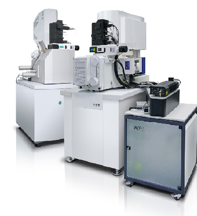
RISE Microscopy is the combination of confocal Raman Imaging and Scanning Electron Microscopy. It incorporates the sensitivity of the non-destructive, spectroscopic Raman technique along with the atomic resolution of electron microscopy. Raman Imaging enables the identification of molecules, their allotropes and polymorphs, the determination of their orientation, purity and crystallinity, and the detection of strain states. SEM allows for the imaging of surface structures on the nanometer scale. RISE combines the advantages of both, thus facilitating the most in-depth characterization of the sample.
The Raman effect is based on the inelastic scattering of light by the molecules of gaseous, liquid or solid materials. The interaction of a molecule with photons causes vibrations of its chemical bonds, leading to specific energy shifts in the scattered light. Thus, any given chemical compound produces a particular Raman spectrum when excited and can be easily identified by this individual "fingerprint."
Raman spectroscopy is a well-established, label-free and non-destructive method for analyzing the molecular composition of a sample.
In Raman imaging, a confocal microscope is combined with a spectrometer and a Raman spectrum is recorded at every image pixel. The resulting Raman image visualizes the distribution of the sample's compounds. Due to the high confocality of WITec Raman systems, volume scans and 3D images can also be generated.
The Raman effect is extremely weak, so every Raman photon is important for imaging. Therefore WITec Raman imaging systems combine an exceptionally sensitive confocal microscope with an ultra-high throughput spectrometer (UHTS). Precise adjustment of all optical and mechanical elements guarantees the highest resolution, outstanding speed and extraordinary sensitivity — simultaneously!
This optimization allows the detection of Raman signals of even weak Raman scatterers and extremely low material concentrations or volumes with the lowest excitation energy levels. This is an unrivaled advantage of WITec systems.
A mineral phase of a rock section from a drill core was analyzed in the next example. The dominant rock type is Diorite. The sample had no need to be treated or vaporized but was only sectioned with a diamond saw under water. This reduces the risk of contamination of the surface, which is of great importance not only for geological drill cores but also for objects derived from the deep sea.
Fig. 1a shows the SEM image of a small sample area using the back-scattered electron detector of the SEM. The same area was analyzed using EDX (Fig. 1b). The distribution of elemental groups indicates the presence of three distinct minerals. Single Raman spectra could be acquired from the three different areas (Fig. 1c), three of which show the characteristic Raman bands for quartz, epidote and plagioclase. This is in good agreement with the elemental composition obtained by EDX. Raman spectra of the three primary minerals were evaluated using cluster analysis. In addition to these spectra, four others were detected, two of which could indicate different grain orientations within the phases of epidote and plagioclase respectively. The spatial distribution of the minerals is shown in the color coded RISE image (Fig. 1d) where the colors of the Raman image match the colors of the spectra. Not only mineral phase distribution could be detected but also small grains within a mineral phase. Fig. 1e shows the white light image acquired from the same sample area as the SEM image. It clearly emphasizes that high resolution optical images require proper focusing, whereas SEM is completely insensitive to surface roughness, which is why it is difficult to retrieve the sample area when using two stand-alone instruments.
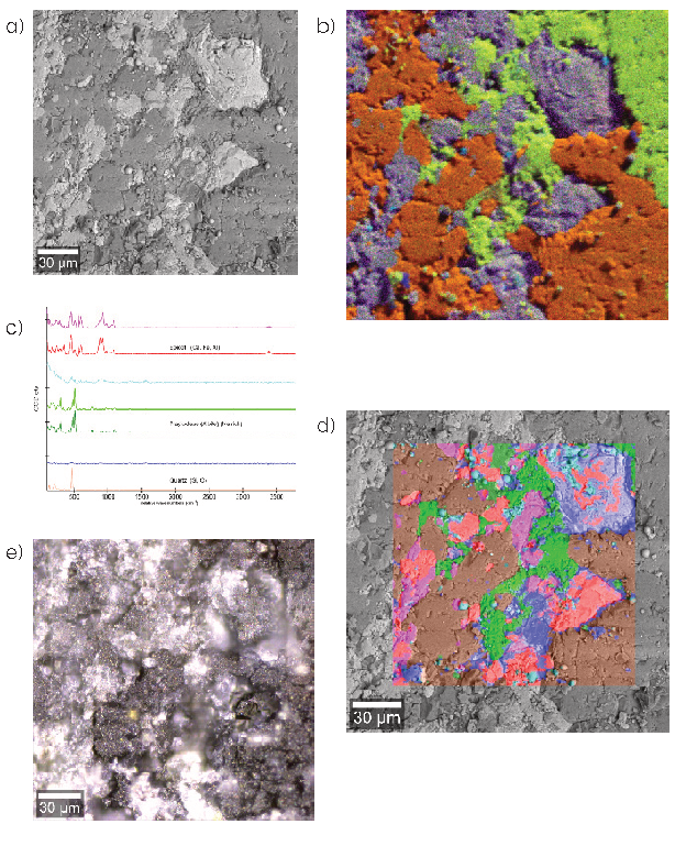
Fig. 1 — A mineral phase of a diorite rock section. (a) SEM image (b) overlay of SEM and EDX image; three element groups distinguished with EDX: Si, O: orange; Ca, Fe, Al: grey-purple; Na: green. (c) Raman single spectra acquired from the three distinct regions with the characteristic Raman bands of quartz (brown), epidote (red) and plagioclase (green). (d) Raman spectral image overlaid with the SEM image. (e) Light-microscopy image from the same sample area. Image parameters: 100 x 100 µm², 150 x 150 pixels = 22,500 spectra, integration time 0.08 sec per spectrum. Sample courtesy of Christiane Heim, Geoscience Centre GZG, Dept. Geology, University of Göttingen, Germany.
Non-conductive compounds can be examined with modern SEMs without specific pretreatment by using a low vacuum mode that prevents the material from being electrically charged. Imaging polymer blends or biological materials in this way can reveal a contrast in the SEM images, though without giving any clue regarding the chemical composition of the various phases. A film of a polymer blend consisting of polystyrene (PS) and polymethylmethacrylate (PMMA) was analyzed by RISE Microscopy. Both polymers are comprised only of the elements carbon, oxygen and hydrogen. With EDX these elements can be identified without revealing how the elements are combined into molecules.
That is however precisely the strength of Raman imaging as the spectra shed light on the chemical nature (structural units, type and degree of branching, end groups, additives), conformational order (physical arrangement of the polymer chain), state of the order (crystalline, mesomorphous, and amorphous phases), and orientation (type and degree of polymer chain and side group alignment in anisotropic materials). Fig. 2 shows an overlay of a color coded RISE image of the PS (green) – PMMA (red) mixture. The SEM image reveals the fine structure of the two polymeric phases, whereas the chemical identification of the polymeric phases is provided by the confocal Raman image.
The Raman spectra of PMMA and PS are shown in Fig. 2b. Due to their different hydrophilic properties the two compounds do not mix but form a dispersion of separated beads.
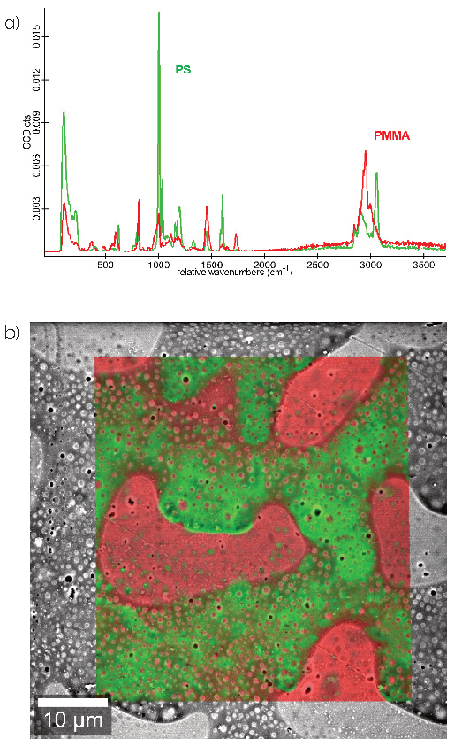
Fig. 2 — (a) PMMA (red) and PS (green) show characteristic, distinguishable Raman spectra. (b) Based on the spectra a Raman image of a PMMA-PS emulsion was taken and overlaid with a SEM picture. Image parameters: 50 x 50 µm², 300 x 300 pixels = 90,000 spectra, integration time 0.035 sec per spectrum.
In this application example RISE Microscopy was performed on a microtome slide of hamster brain tissue. In the SEM image the white and gray brain matter can be distinguished by their structural differences. Both tissues can be also chemically distinguished by their typical Raman spectra (figure 3a). Overlaying the SEM with the color-coded Raman image reveals a more precise view of the distribution of the gray and white matter (figure 3b).
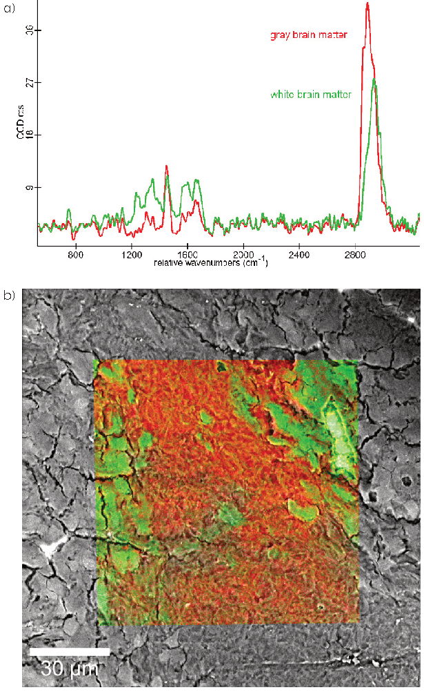
Fig. 3 — (a) The Raman spectra of a hamster brain tissue sample reveal the different spectral characteristics of the white and gray brain matter. (b) Raman-SEM image overlay. In the color-coded Raman image the white brain matter is shown in green and the gray brain matter in red. 100 x 100 µm², 300 x 300 pixels = 90,000 spectra, integration time: 50 ms/spectrum.
Thin-layered or single layer materials, defined as 2D materials, have recently attracted enormous research interest due to their special electronic and optical properties which differ significantly from that of their bulk precursors. Graphene is one of the most popular materials extensively studied in this context. In Fig. 4 the SEM (a) and RISE (b) images of a CVD graphene sheet deposited on Si/SiO₂ substrate are presented. The SEM image was acquired with low acceleration voltage (2 kV) using the secondary electron (SE) detector. This imaging mode of the SEM is very surface sensitive, thus revealing the fine structure of the CVD graphene sheet. The colors used represent a single layer (blue, dark green) with different grade of defects and more than one layer (light green, red). The RISE image highlights the large amount of defects in the blue area, in good agreement with the high resolution SEM image.
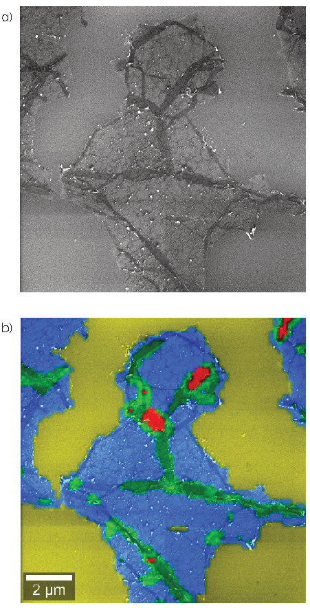
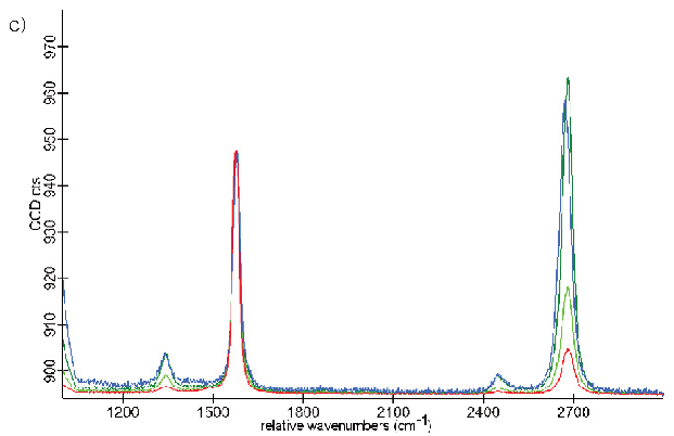
Fig. 4 — (a) SEM image of a graphene sample. (b) SEM image overlaid with the color-coded confocal Raman image. The colors display the graphene layers and wrinkles. Image parameters: 20 x 20 µm², 150 x 150 pixels = 22,500 spectra, integration time: 0.05 s/spectrum. 1 layer (blue, dark green), >1 layer (light green, red), Si (yellow).
The special properties of carbon nano-tubes such as high thermal conductivity make them interesting for applications in electronics, nanotechnology, optics and materials science. Single-wall carbon nanotubes (SWCNTs) consist of a single atom thick, curved sheet of carbon. Their unique electronic and mechanical properties make them attractive for electronics fabrication. The Raman spectrum identifies SWCNTs as single-walled by the presence of their characteristic RBM (radial breathing mode) bands at low wavenumbers (fig. 5a). The RISE image (fig. 5c) of SWCNTs embedded in polyethylene (PE) was generated by merging the Raman image (fig. 5b) with the SEM image.
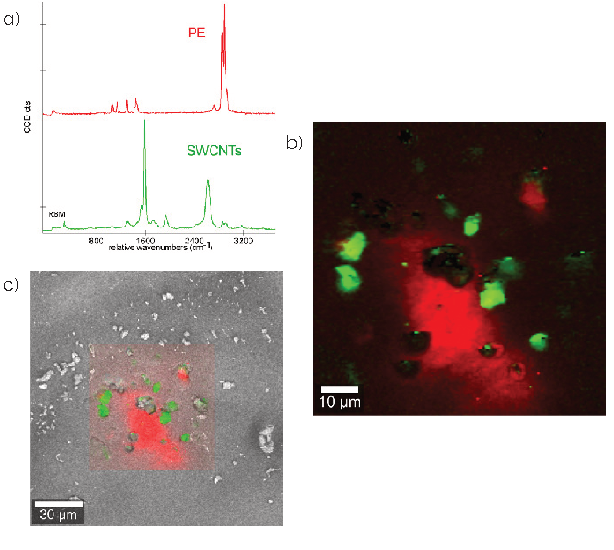
Fig. 5 — (a) Characteristic Raman spectra of SWCNTs and PE. (b) Color-coded Raman image. (c) RISE image. Image parameters: 150 x 150 µm² scan range, 80 x 80 pixels = 6,400 spectra, integration time: 60 ms/spectrum. PE (red), SWCNTs (green), SEM image (grey).
Volume scans are a valuable tool in providing information about the dimensions of objects or the distribution of a certain compound throughout the sample. In order to generate 3D images, confocal 2D Raman images of different focal planes are acquired by scanning throughout the sample in the z-direction. The 2D images are then combined into a 3D image stack. To explore the 3D structure of the SWCNTs sample, 16 Raman images were taken in the z-direction intervals of 1 µm (fig. 6a). From these data a 3D image was compiled. It illustrates that the SWCNTs lie on top of the PE matrix (fig. 6b).
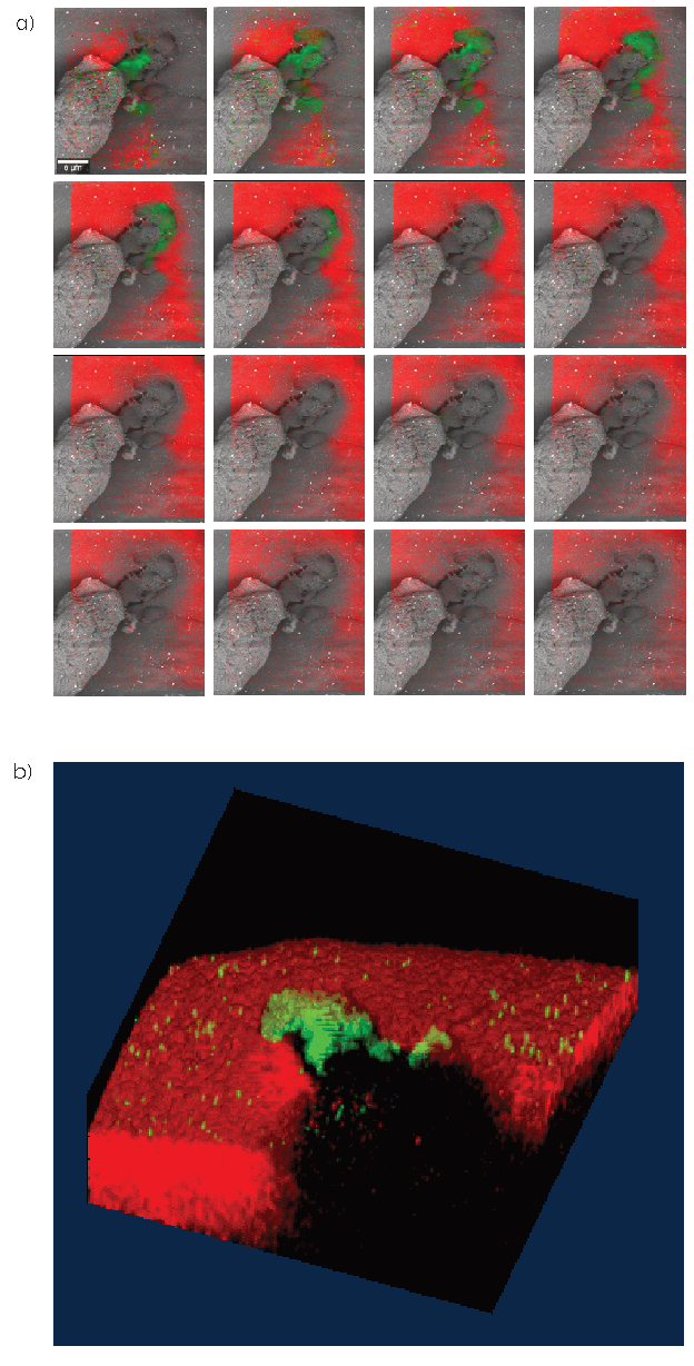
Fig. 6 — 3D imaging of SWCNTs on PE film. For a 3D image of the SWCNTs on PE sample, 16 equidistant Raman images were taken while the focus was shifted by 1 µm for each image. The individual images are displayed as RISE images in (a). The compiled 3D Raman image of the analyzed sample area shows the SWCNTs located on the top of the PE filter (b). Image parameters: 200 x 200 µm² scan range, 70 x 70 pixels = 4,900 spectra, integration time: 0.037 s/spectrum. PE (red), SWCNTs (green), SEM images (grey).
Inspired by progress in graphene research, other mono-layered materials such as hexagonal boron nitride (h-BN) and transition metal dichalcogenides (TMDs) have also received widespread attention. Recent work has shown that exfoliated monolayer molybdenium disulfide (MoS₂) is a 2D direct bandgap semiconductor indicating that the material is suitable for optoelectronics and energy harvesting. Bulk MoS₂ however is an indirect bandgap semiconductor. Thus detailed knowledge of the structures and features of grains and grain boundaries are essential for understanding and exploring the materials' properties and its further applications. Here we present with MoS₂ that RISE microscopy reveals structure as well as crystalline and exciton dynamics of thin-layered TMDs.
CVD grown monolayers of TMDs form triangular two dimensional crystals. Twin crystals of MoS₂ on SiO₂/Si appear in the SEM image as star-shaped forms (fig. 7a). The Raman spectra of these 2D crystals show the characteristic E2g and A1g Raman band modes of MoS₂ (fig. 7c). With an increasing number of layers the two Raman bands drift apart due to inter-layer and in-plane vibrations. At the grain boundaries the Raman bands not only show shifts, but additional bands also appear (green spectra), indicating defects or misaligned 2D crystals. They probably result from adjacent crystals colliding out at their boundaries. The spectral information was used to create a Raman image which was overlaid on the SEM image (fig. 7b). The overlapping boundaries identified by Raman imaging correlate perfectly with the dark edges visible in the SEM image.
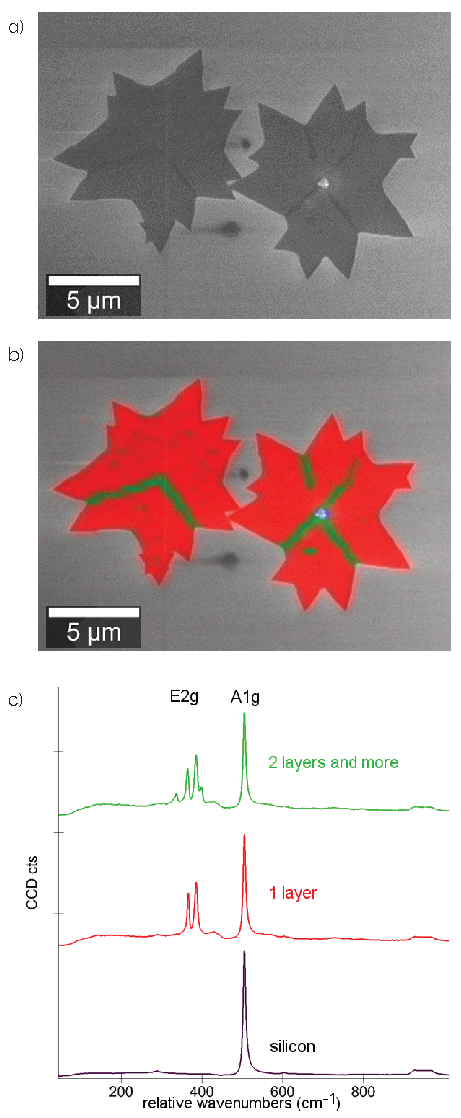
Fig. 7 — (a) SEM image of MoS₂ twin crystals. (b) Corresponding color-coded Raman image derived from the spectral information overlaid on the SEM image to give the RISE image. (c) Raman spectra of MoS₂ monolayers (red), two or more layers (green) and silicon (purple). Image parameters: 22 x 17 µm² scan range, 65 x 50 pixels = 3,250 spectra, integration time: 0.037 s/spectrum.
With SEM it is possible to identify materials consisting of different atoms using a common combination with EDX (energy-dispersive X-ray spectroscopy). It cannot however distinguish between different materials (polymorphs). As the manner of atomic bonding greatly influences the structure and properties of a material, visualizing not only morphology but also identifying its molecular architecture is important. RISE microscopy accomplishes both of these tasks as demonstrated with the analysis of TiO₂ polymorphs (fig. 8). TiO₂ is studied intensively because of its interesting chemical and optical properties and is widely employed in photo-catalysis, electrochemistry, photovoltaics and chemical catalysis. It is also used as white pigment in tooth paste, sun screen and wall paint and as anode material for lithium-ion batteries. Depending on the application, one crystalline form or the other gains in importance.
TiO₂ occurs in eight modifications, two of which — anatase and rutile — were examined. For RISE microscopy an SEM image was taken of a 1:1 anatase/rutile powder mixture (fig. 8a). The corresponding confocal Raman image from the same sample area was merged with this SEM image (fig. 8b). It was demonstrated that though the elemental compositions of the modifications anatase and rutile are identical, they can be distinguished from one another by their characteristic Raman spectra at relative wavenumbers between 300 and 800 cm⁻¹ (fig. 8c). Both phases were combined in agglomerates, in which rutile accumulated in larger particles than anatase.
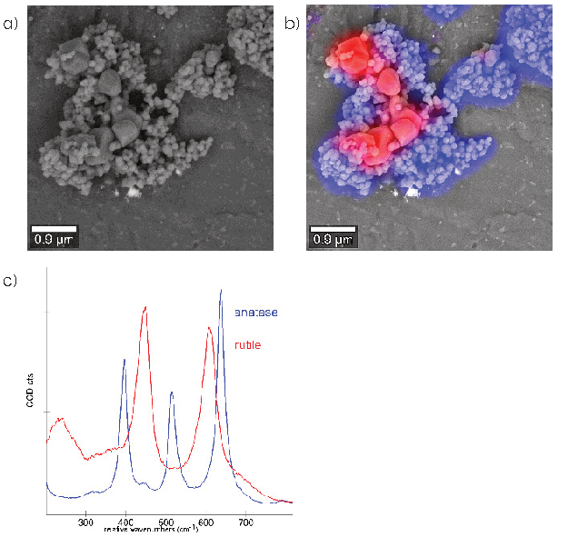
Fig. 8 — Two modifications of TiO₂, anatase and rutile, were mixed 1:1, ground, dissolved in water and imaged with an SEM (a) and a confocal Raman microscope. (b) SEM and Raman images overlaid. (c) In the Raman spectrum anatase (blue) can be easily distinguished from rutile (red). Image parameters: 12 x 12 µm² scan range, 150 x 150 pixels = 22,500 spectra, integration time: 0.037 s/spectrum.

© Oxford Instruments 2026